Answer

Trace for flop_ops
Types of Operators
In the given program, operations other than matmul are bottlenecked on memory bandwidth - how fast we can read and write from DRAM - and not compute. When root causing the performance bottleneck, here’s some things that stand out:
- Summing matrix elements takes roughly half as long as multiplying a scalar into the matrix.
- The operations
sqrt,sin,sigmoid,log10,powtake roughly the same time as scalar multiplication. - Adding two matrices takes roughly $50\%$ longer than scalar multiplication.
A key observation is that there are three types of operations happening above:
- Reduction e.g., summation, we read entries only once from DRAM (the sum is “accumulated” in local registers), for scalar multiplication, we read and write back entries.
- In-place point-wise operation e.g., scalar multiplication requires one read and one write.
- Out-of-place point-wise operation e.g., adding matrices requires two reads and a write for each entry in the result.
GPU Memory Bandwidth
Before the GPU can perform numerical operations on data, that data has to first be read into registers. The peak memory bandwidth for a A100 (40 GB) is $1.555$ TB/sec. This means that an $8192 \times 8192$ matrix of FP32 values takes at least $4 \times (8192)^2/1.555e12 = 0.17$ ms to read. Therefore,
- Even if numerical operations took no time, scalar multiplication takes at least $0.34$ ms (read, write back)
- Scalar multiplication achieves $0.197$ TFLOPS/sec $\sim 1\%$ of the advertised FP32 flops.
Flops per Operation
From CPU-side profiling, we can estimate the number of flops the GPU uses to perform math operations:
sqrt($7$),sin($3$ single precision, $14$ double precision),sigmoid($24$),log10($24$),pow($142$).- For all of these, except
pow, we are strongly dominated by memory bandwidth.
Matrix multiplication achieves $19.5$ TFLOPS/sec. This is because once we read in a value, we operate on it multiple times, amortizing the cost of the read.
Discussion
What is arithmetic intensity?
The ratio of flops performed by an operation to the bytes read/written is known as the arithmetic intensity of the operation.
What is the arithmetic intensity for matrix multiplication and point-wise operations?
For matrix multiplication of two $n \times n $ matrices, the flop count is $O(n^3)$, and when planned carefully the number of bytes read/written are $O(n^2)$ so the arithmetic intensity is $O(n)$.
For point-wise operations, the flop count is $O(n)$, where $n$ is the number of tensor entries; the bytes read/written is also $O(n)$ so the arithmetic intensity is $O(1)$.
When is an A100 (40 GB) memory bandwidth bound?
An A100 (40 GB) can perform roughly $50$ flops in the time it takes to read or write $4$ bytes (single precision float). If the arithmetic intensity of a program < $50$ on an A100 (40 GB) then it will be bound by memory bandwidth.
How do you explain the advertised FP32 performance (19.5 TFLOPS/sec) from the A100 microarchitecture?
The maximum clock speed of an A100 is $1410$ MHz. Dividing the advertised flops by the clock speed, we get $13830$ FLOPS/cycle. Looking at the spec sheet, we see it has $6912$ “CUDA Cores” - this number is suspiciously close to $13830/2 = 6915$.
A CUDA Core is essentially one single precision floating point unit. Multiplying two n-bit numbers entails adding n-1 partial products. Therefore a MAC (multiply-and-accumulate) operation has very little incremental cost over multiplication. All hardware vendors consider a MAC to be two flops - so $6912$ cores can perform $13824$ FLOPS/cycle. The discrepancy with $13830$ above is due to rounding.
Even for compute-bound workloads achieving peak flops is hard - every CUDA Core has to perform a MAC every single cycle.
Can peak memory bandwidth be achieved on an A100 (40 GB)?
Just like TFLOPS/sec, the memory bandwidth on GPU spec sheets can easily be misunderstood. It corresponds to best case memory layouts i.e., when copies are aligned with cache dimensions. The high memory bandwidth is due to a very wide memory bus ($5120$ bits) which is roughly $10 x$ that of a CPU. It is optimal for reading/writing to/from long contiguous segments of memory.
While reading/writing tensors are an ideal use case some challenges still remain. E.g., consider the case of transposing a 2D matrix - if the matrix is read in column major order then a naive approach to writing the result will be fragmented. The solution is to use clever memory access by coalescing reads and using shared memory.
What should you remember in years to come?
Though we focus on compute, GPUs have additional performance constraints. Arithmetic Intensity i.e. the ratio of flops to bytes read/writtten; is the key to determining if a program is compute or memory-bandwidth bound on a GPU and users should strive for higher arithmetic intensity in the kernels.
Explore more
How can arithmetic intensity be measured for a kernel?
An approximation can be derived using the tensor shapes and kernel duration from the PyTorch Profiler trace. For a more precise answer we recommend using NSight Compute (NCU) which creates a roofline plot for the kernel. Moreover, NCU also provides a memory chart which aids in identifying hotspots in the memory subsystem.
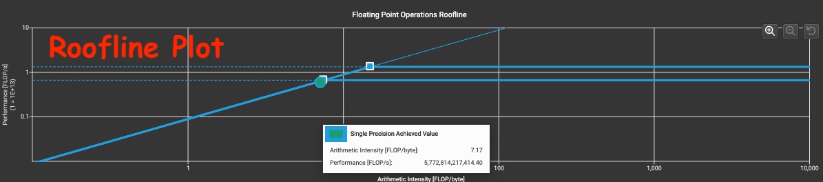
Roofline Diagram
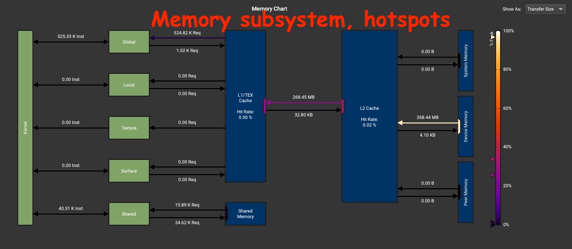
Memory Subsystem
How do you compute the flops needed by a program?
Use perf stat to get CPU-side flop count. The code snippet below calcuates the $sin$ of a tensor
and then uses perf stat to calcuate the number of floating point operations at various precision
levels.
import torch
random_data = torch.rand((1000000,), device='cuda')
sin_data = torch.sin(random_data)
perf stat -e fp_arith_inst_retired.256b_packed_double python3 sin.py
perf stat -e fp_arith_inst_retired.256b_packed_single python3 sin.py
perf stat -e fp_arith_inst_retired.512b_packed_double python3 sin.py
perf stat -e fp_arith_inst_retired.512b_packed_single python3 sin.py
perf stat -e fp_arith_inst_retired.scalar_double python3 sin.py
perf stat -e fp_arith_inst_retired.scalar_single python3 sin.py