Answer
Puzzler 1
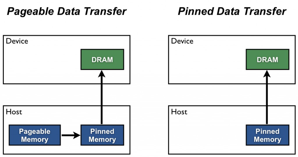
Direct Memory Access (DMA) is a feature by which hardware subsystems (GPU, NIC, drive, etc) can access host-memory without going through the CPU. Without DMA, we have “CPU bounce” - the CPU has to read from host-memory and write to the PCIe bus. This slows down the transfer and also keeps it from doing other work (the extent of the slowdown depends on how fast the CPU is). Therefore it’s advantageous to use DMA.
Host side memory comes in 2 flavors:
- pageable
- pinned (a.k.a. page-locked)
DMA can only be applied to pinned memory.
It’s easy to pin memory in PyTorch. Acpu = torch.rand(N).pin_memory() does the trick. With this the
transfer speed almost triples to 12 GB/sec.
Puzzler 2
GPU memory is allocated and freed by calls to cudaMalloc() and cudaFree(). cudaMalloc() and
cudaFree() cause device-to-host syncs, which in turn result in the launch queues emptying, exposing
kernel launch overhead. PyTorch uses the CUDA Caching Allocator (CCA) to overcome this. It holds on
to memory allocated by cudaMalloc() and recycles it. Critically, CCA is smart enough to recycle
memory allocated for the single stream case.
Let’s say in iteration $i$, the CCA chooses GPU memory GPU_ptr_0 for storing Asquare. When
iteration $i+1$ begins, the Python runtime will have executed the destructor for Asquare from
iteration $i$ since the Asquare tensor went out of scope at the end of iteration $i$. This happens
before the next constructor call for the Asquare object in iteration $i+1$.
Here’s the above argument applied to the test program:
for i in range(3000):
  #  Consider iteration 100
  Asquare = torch.matmul(A,A)  # Say 0x6000 is the address of Asquare.
  # iteration ends
  # => Asquare goes out of  scope
  # => Tensor destructor called, has CCA callback
  # => CCA knows 0x6000 is available
  # Verify recycling by looking at Asquare.data_ptr
A big thanks to Andrew Gu and Zachary DeVito for providing clarifications on this material.
Puzzler 3
One reason for transpose()’s poor performance is the fact that it’s launching kernels in a loop -
looking at the timeline trace, there are huge gaps, coming from kernel launch overhead, between the
copy kernel calls that perform result[i,:] = A[:,i].
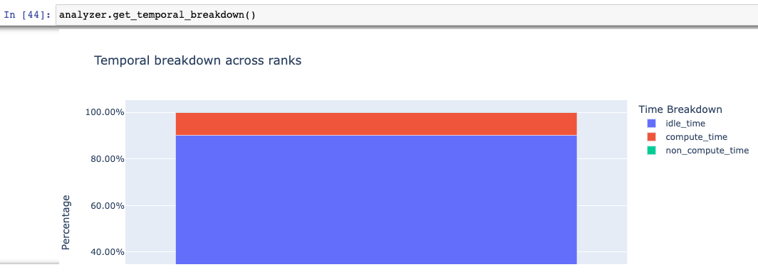
Using Holistic Trace Analysis, we see that the GPU is 90% idle.
Matrix transpose does not perform any computation - it’s just moving bytes around. We read and then
write $4 \cdot 4096^2$ bytes in $173$ ms. Discounting the gaps from kernel launch, the naive
transpose() takes $17$ ms, so the effective memory bandwidth transpose() achieved is $8$ GB/sec.
More precisely, $4 \cdot 4096^2$ bytes read and $4\cdot 4096^2$ bytes written in $17$ ms.
An A100 has $\approx 1.5$ TB/sec memory bandwidth, so we have a gap of almost $200 \times$ ($1.5$
TB/sec / $8$ GB/sec) to explain. Recall peak memory bandwidth comes when we move large ($5120$ bits)
contiguous blocks of memory. This is definitely not the case with transpose - specifically, there is
a lot of fragmentation on the read side since torch tensors are row major and A[:,i] is a column.
There are several optimizations that can be performed to improve the performance of transpose - these all have to happen at the level of a CUDA kernel - they are not available from PyTorch. The two key optimizations are:
- Memory coalescing - load contiguous blocks from off-chip DRAM into the on-chip SRAM (the shared memory (SMEM)), and perform operations in SMEM, which is faster and doesn’t require very wide memory accesses to get peak bandwidth.
- Bank conflict minimization - SMEM is made of individual banks of SRAMs, and each bank can support only a single read/write per cycle, so it’s important to place data to minimize concurrent accesses to a bank.
We give details on both of these in the discussion section.
Discussion
Why does DMA require pinned memory?
Paged memory access requires the ability to translate virtual to physical addresses, which requires a Memory Management Unit (MMU) which is on the CPU). For DMA to work, we need physical addresses, since there’s no MMU - this is why the memory must be pinned. (link)
Why does the copy not achieve the full 16 GB/sec we’d expect from PCIe v3?
It’s due to a combination of protocol overhead and contention (the CPU connects to multiple devices through the same PCIE bus).
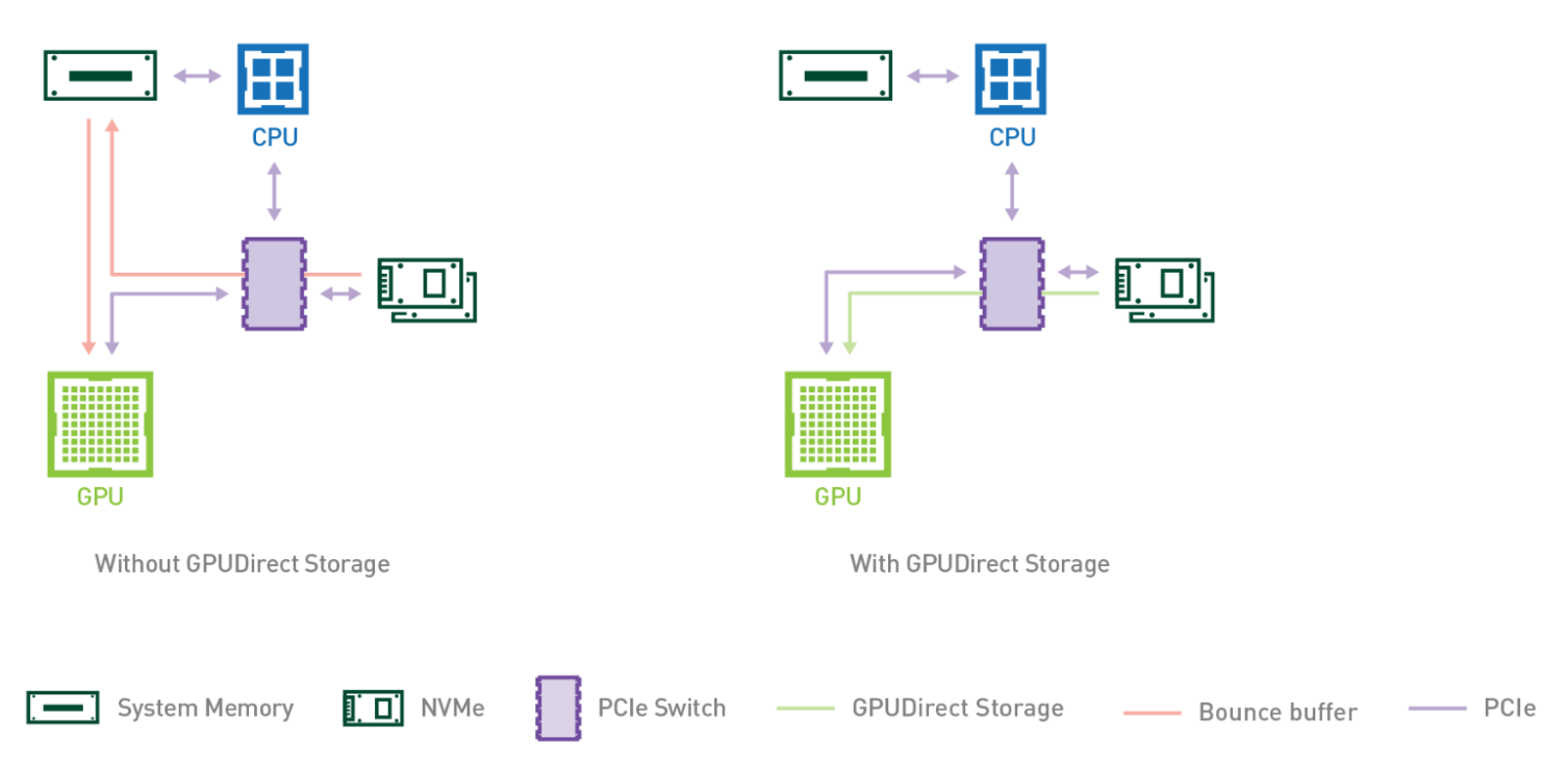
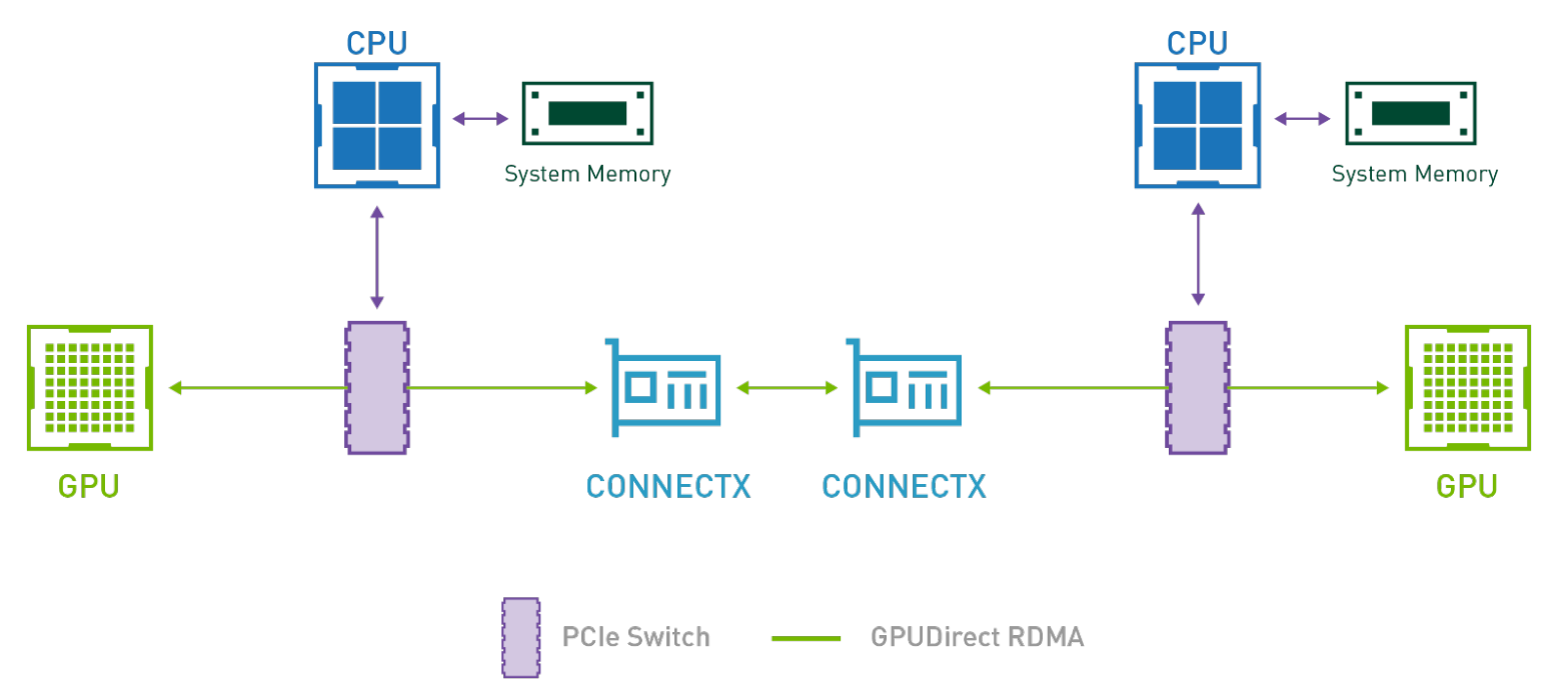
How does this relate to GPUDirect Storage and GPUDirect DMA?
As previously discussed, CPU bounce is a performance killer when copying from host memory to GPU and can be avoided using DMA. In the same spirit, copying directly between peripherals such as NICs and video acquisition devices and GPU is beneficial. GPUDirect RDMA enables direct data exchange between GPUs and a third-party peer device using PCI Express. GPUDirect Storage is a specialization for communicating with storage devices Learn more about GPUDirect RDMA and GPUDirect Storage.
Where do cudaMalloc() and cudaFree() run?
Both run on the host - the CUDA context on the host has complete knowledge and control of memory on the GPU.
It seems counter-intuitive that memory can be reclaimed before it’s even been used?
The key is to realize that the CCA serves as a middle layer to orchestrate which GPU memory a kernel will use when it actually runs. This orchestration can be planned long in advance (in the case of a fast CPU thread). It doesn’t matter if the GPU has actually performed the operation - kernels are strictly ordered within a stream, so CCA will know that the memory will be free when the ops that consume the requested allocation execute. Therefore, CCA knows that it can reuse those blocks. Operationally, there will be a call in the tensor’s destructor to the CCA (in practice, there’s an intermediate call to the storage implementation).
What will happen if we were to record the result of each squaring, e.g., by appending each Asquare to a list?
CCA will not reclaim storage, and the program will OOM.
What happens when a tensor is produced by a kernel in one stream and then input to a separate kernel in another stream?
When used across multiple streams, the GPU memory block cannot be marked as okay to reuse until the block’s cross-stream usage finishes on the GPU. Tracking this is the responsibility of the application, and it can be challenging. For example, it’s possible for the producer to overrun the consumer, resulting in OOMs. (The solution is to use rate limiting, i.e., keep the queue from becoming too big, see this paper for details.)
What is memory coalescing?
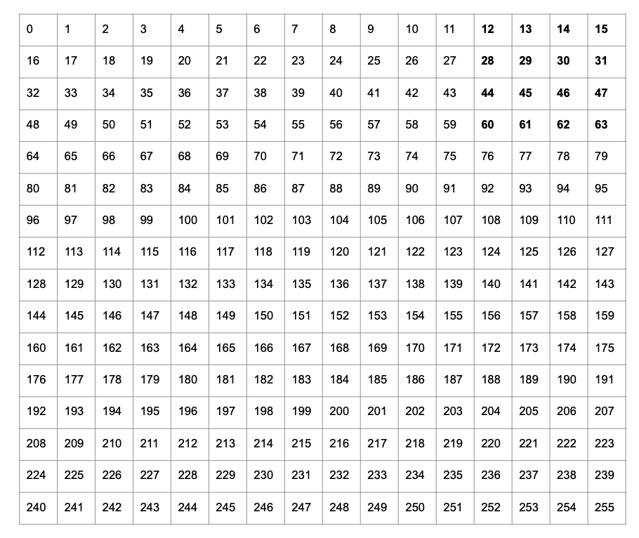
Consider a 16x16 matrix as shown below.
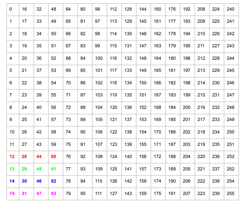
RAM is one-dimensional, so the actual memory layout of this matrix is shown below. (PyTorch uses “row-major” order.)
Recall that a GPU has very high peak memory bandwidth but this is only achieved when reading large contiguous blocks of memory (since the memory bus width is very high). Naive transpose reads entries $0-15$, and writes to indices $0, 16, 32, \ldots 244$. Since none of these writes are contiguous, naive transpose is slow. (If we wanted to make the writes contiguous, e.g., by writing the result row-by-row, we’d have to read from indices $0, 16, 32, \ldots 244$ from the original array.)
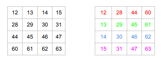
The GPU also has very fast, though relatively small, on-chip SRAM known as Shared Memory (SMEM). In addition to being fast, SMEM has a relatively narrow memory bus. We can read in a $4 \times 4$ submatrix, e.g., the top-right entries shown in boldface, and transpose them in the SMEM, as shown below.
Now we can write the submatrix to the result. In particular, we only need 4 contiguous writes for this submatrix, which are coded in color.
What are bank conflicts?
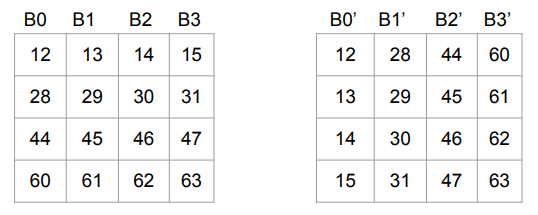
In reality, shared memory (SMEM) is not a true monolithic RAM - it’s composed of multiple memory “banks” to achieve high bandwidth. So the picture is closer to the following, where B0, B1, B2, B3 are the different memory banks.
We cannot efficiently generate the first row of the result, since that means we need to perform 4 reads out of B0; nor can we efficiently generate the first column of the result, since that entails 4 writes into B0.
However, we can “stagger” reads and writes to create a schedule that’s free of bank-conflicts. The colors encode which values are written in a specific iteration.
These enhancements are enough to get transpose performance near roofline. This may sound surprising, since we are doing 2 reads and 2 writes per element. However, one of the reads and one of the writes is in the SMEM, which is very fast. Furthermore, SMEM read/write latency can be effectively hidden by overlapping with HBM reads/writes.
General Memory Movement Optimization
Optimizing memory access is one of the most challenging aspects of CUDA programming. For example, when we computed the arithmetic intensity of square matrix multiplication, we wrote it as $\frac{2n^3}{3w \cdot n^2}$, where $n$ is the matrix dimension and $w$ is the word size.
The justification we gave was that to compute $A = B \times C$, we need to read each element of $B$ and $C$, and write each element of $A$. However, if you look at the expression for the result, you’ll see each element of $B$ and $C$ is read multiple ($n$) times!
\[A_{0,0} = B_{0,0} \cdot C_{0,0} + B_{0,1} \cdot C_{1,0} + \ldots + B_{0,n-1} \cdot C_{n-1,0}\] \[A_{0,1} = B_{0,0} \cdot C_{0,1} + B_{0,1} \cdot C_{1,1} + \ldots + B_{0,n-1} \cdot C_{n-1,1}\] \[\vdots\]It’s through clever use of the memory hierarchy (including the coalescing and banking techniques) that we can get away with $n^2$ reads from $B$ and $C$ respectively. This page summarizes the GPU memory hierarchy and here’s an example of developing a fast GEMM.
Transpose in O(1) time
Remarkably, A.transpose(0,1) is an $O(1)$ operation. The reason for this is that it simply updates
the “strides” in the (host-side) tensor object for $A$. To be precise, an $m$-dimensional tensor $T$
contains a length $m$ tuple of “strides” ($s_1,s_2,\ldots s_m$). The entry $T[i_1] [i_2] \ldots [i_m]$
is at entry $s_1 \cdot i_1 + s_2 \cdot i_2 + \dots + s_m \cdot i_m$ in the 1D array that stores
$T’s$
entries. For an $n \times n$ matrix $A$, $s_1=n,$ and
$s_2=1$. Using $s_1=1$ and $s_2=n$ has the effect of transposing $A$.
What should you remember in years to come?
GPU memory access patterns plays a critical to PyTorch performance. It’s important to have a good mental model of the GPU memory hierarchy.
Explore more
- NVIDIA Blog on Efficient Matrix Transpose (memory coalescing and removing bank conflicts)
- NVIDIA Memory Optimizations course
